
Board Manufacturing
 R&D Altanova is the leading supplier of A.T.E. products to some of the world’s largest semiconductor manufacturers and fabless semiconductor companies. Since R&D began manufacturing semiconductor test boards over 20 years ago, it has grown to be the core competency of our company. R&D Altanova plans and equips its Design, Manufacturing and Assembly facility capabilities expressly in support of the needs of our A.T.E. customers. We utilize the most commonly asked-for software packages for A.T.E. board design in order to support your company with the format that suits it best. Our production facility has maintained and purchased new equipment to consistently meet the challenges facing our customers today and enable them to plan for the needs of tomorrow.
CURRENT A.T.E. CHALLENGES:
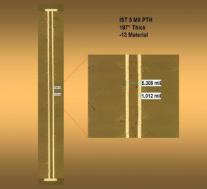
High Aspect Ratio – R&D Altanova regularly manufactures boards with aspect ratios of 35:1 and more. This has become a proven technology, based on our consistent testing with the Interconnect Stress Test methodology. R&D Altanova has expanded our high-speed drilling capabilities with multiple high-speed drill machines. X-ray drilling and laser drilling and routing are also available. Aspect Ratios are available beyond 35:1, though R&D recommends utilizing our expert engineering staff. With their collective years of experience, they can assist you in designing the best possible manufacturing yields and means of maintaining competitive pricing.
Signal Integrity / Signal Performance Loss – Our SI/PI engineering team and our design engineering team have a unique advantage, since we offer all these services, and more, under one roof. They know the board fabrication facility’s capabilities – cold. We don’t have to design to general specifications while you shop around for someone to fabricate your boards, we can design your test needs within the capabilities of our own fabrication facility. Solving problems with stack-ups, material choices, drilling capabilities and the like; we *know* what we can do and we make it happen.
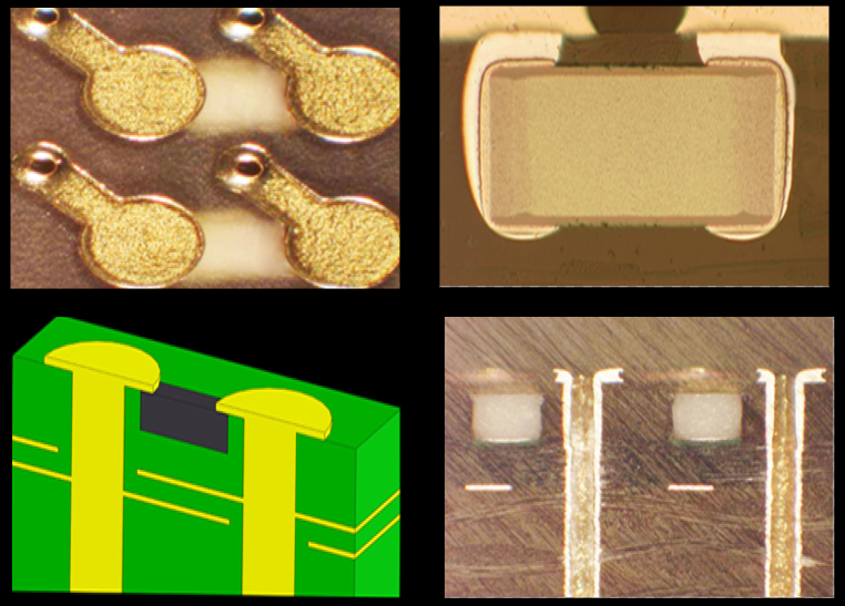
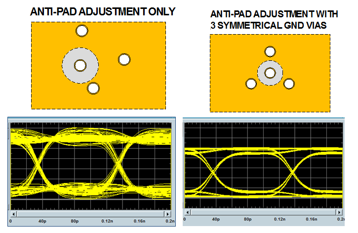
One example of that capability is with regard to improving the fidelity of via’s that are an inevitable part of printed circuit design and manufacturing. There are some techniques that can be employed to assist with improving the response of those via’s as shown below: making adjustments to the anti-pad in the plane layers in a board is one way, as seen in the left example; a second example is to the right, depicting the strategic (calculated) placement of ground via’s surrounding a center signal pin. Each of these is fine for use with lower speed digital applications, less than around 10 Ghz.
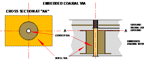
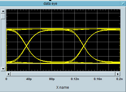
A unique method for improving the signal performance is the use of embedded coaxial via’s as seen below. It is a signal via embedded within a ground sleeve, right inside the board. And, as evidenced by the eye diagram, significantly better response by the coaxial via.
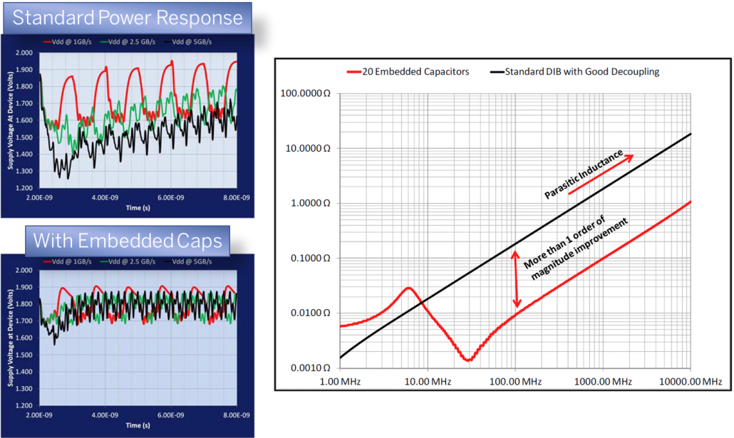
Power Delivery Performance – Planes not meeting expectations? Power droop caused by multi-site test draining tester resources? R&D Altanova has a solution for you. Our EC Technology™ will put power where you need it, by embedding components in the board, at the critical delivery locations your test needs. Embedding passive components inside a PWB is not new, it has been around for twenty years and we have been doing it for at least ten years. By adding capacitors inside the PWB at locations directly under the DUT, you should see dramatic improvements in response time. By adding resistors, you can terminate right at the pin location and not have to find room on the surface for that same resistor. That’s right, these components are off-the-shelf…not specially made.